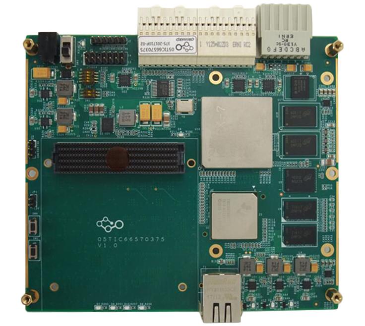
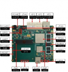
375-Image acquisition and processing platform based on TMS320C6657+FPGA-K7 Brief introduction

Item No.: 375
The DSP+FPGA high-speed signal acquisition and processing board is independently developed by our company, including a TI DSP TMS320C6657 and a Xilinx K7 FPGA XC7K325T-1FFG900.
Description
Overview
The DSP+FPGA high-speed signal acquisition and processing board is independently developed by our company, including a TI DSP TMS320C6657 and a Xilinx K7 FPGA XC7K325T-1FFG900. It includes 1 Gigabit Ethernet port and 1 FMC HPC interface. It can be used with AD FMC sub-card, image FMC sub-card, etc., for software-defined radio system, baseband signal processing, wireless simulation platform, high-speed image acquisition, processing, etc. The board is shown in Figure 1.
 
Figure 1: High-speed signal acquisition and processing platform
 

Figure 2: Block diagram of the image processing platform

1.1.Processing board specifications 

 TI's TMS320C6657 and xilinx's K7 series FPGA XC7K325T-1FFG900 are the main chips.
DSP plug-in DDR3, 128M*32bit capacity;
Nor Flash 16M x16bit capacity;
4Gb NandFlash
Outgoing 1 Gigabit Ethernet interface;
The DSP is connected to an external EEPROM.
The DSP and K7_325T are directly interconnected via RapidIO x4 mode, supporting 4 x 2.5 Gbps / 4 x 5 Gbps;
FPGA external 32M BPI Flash;
FPGA external 1 set DDR3, a total of 128MX32bit capacity;
FPGA and DSP via Rapidio X4, SPI, GPIO, McBSP, uPP, UART;
The connector leads to GTX x 4, LVDS, RS232 for FPGA, PCIEx2 and HyperLink for DSP.
Reset function.
The FPGA is connected to an external HPC high-speed signal interface, and the full signal standard is defined.
Industrial-grade design.

1.2.Physical characteristics

Operating temperature: commercial grade 0°C ~ +55°C, industrial grade -40°C~+85°C

Operating humidity: 10%~80%

1.3.Power supply requirements

Single-power supply, power consumption of the whole board: 20W

Voltage: DC +12V, 5A

Ripple: ≤10%

Fields of application
 Radar, software-defined radio, image data acquisition, radio and television, etc.


2. Hardware description

2.1. Introduction to board resources

This board mainly has two high-speed processors, which are DSP_C6657 and FPGA_325T. Among them FPGA_325T manage the board's power-on timing, clock configuration and reset system. The board resources are shown in the following figure:


Figure 3: An introduction to the image processing platform
Table 1: Image Processing Platform Hardware Parameters - DSP
Processor TI dual-core processor TMS320C6657, supporting fixed-point, floating-point arithmetic, and the main frequency is 1.0GHz
Emulator interface 1x14Pin Rev B JTAG interface, pitch 2.54mm
DDR3 plug-in for DSP MT41J128M16HA-125128M x 32bit =512MB
DSP plug-in Flash JS28F256P30
Nand Flash MT29F1G08ABCHC1Gb  
SPI Flash N25Q128A11BSF40F16MB
EEPROM STMicro_M24M01-HRMN6TP
Internet Ethernet10/100/1000adaptive
Reset mode XC7K325T  Control reset
 
Table 2: Image Processing Platform Hardware Parameters - XC7K325T
Processor Xilinx Kintex-7XC7K325T-FFG900-2I
Emulator interface 1x 6Pin JTAG port, pitch 2.54mm
Startup mode 1 x 4-digit DIP switch, default BPI mode
DDR3 MT41K256M16JT-125256M x 32bit = 1GB
Nor Flash PC28F00AP30TF128M
Serial One road RS232
LED 4 x User Programmable Indicators


Finished product inspection report
Product name High-speed data processing core board based on TI DSP TMS320C6657 and XC7K325T
Product number 05TIC66570375
Lot number  
Thename of the customer  
 
Item Requirement Result
1 Visual inspection
2 Power supply test
3 Test download link test
4 DSPconfiguration, DDR3, indicator function test
5 DSP EEPROM test
6 DSP NorFLASH test
7 DSP NandFLASH test X(The interface function is being debugged)
9 DSP EMIF Nor Flash Boot
10 DSP Ethernet testing
12 FPGA DDR3 test
13 BPI Schema loading
16 DSP- Kintex7 Connectivity testing SRIO_2.5G
17 DSP- Kintex7 Connectivity testing SRIO_5G
19 Inspection of packaging, accessories, instructions
     
Tested By Approved By Data
Li He Jiao Xiaofeng 2018.3.22