


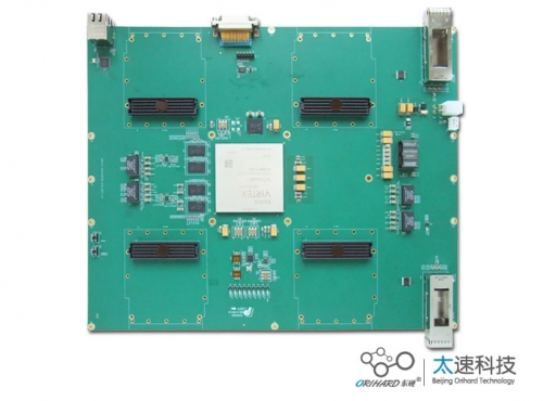
一、PCBA overview The multi-core processor multi-input chip verification board based on XCVU440-FLGA2892 is used to verify network switching chips, including 4 FMC interfaces, DDR, GPIO, etc. This board is used to complete Party A’s chip verification tasks and multi-task functional verification.  Figure 1.1 Verify board schematic block diagram 二、PCBA technical indicators 1) FPGA is externally connected to 4 channels of FMC-HPC. Each FMC supports GTH x8, LA, HA and HB interfaces. The GTH pin distribution of a single group should not span the FPGA Bank. It is recommended to decentralize the board layout to make it easier to adapt to daughter cards. 2) The FPGA is connected to 2 external QSFP+ interfaces. 3) FPGA is externally connected to 1000BASE-T Gigabit Ethernet. 4) There are two sets of DDR3 chips outside the FPGA, each with a capacity of 256M×16, a total of 3 chips, 40bit. 5)The NorFlash capacity mounted on the FPGA must be at least 256MB. 6)The FPGA loading mode is BPI mode. 7)FPGA reserves User IO, at least x80, and some of it needs to be pulled up. 8)FPGA supports JTAG debugging. 9)FPGA supports system reset button. 10)Indicator light display (power input indicator light, FPGA loading complete indicator light, FPGA programmable indicator light). 11)The board requires industrial-grade chips. The structure meets the seismic requirements. 12)The board provides a heat sink, +12V input DC power supply, and overcurrent, overvoltage, and connection protection. 13)PCBA dimensions: 310mm×250mm×18mm |
