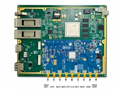
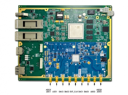
522-four-channel 1G bandwidth satellite data link development platform based on AD9988

Item No.: 522
Satellite communication is one of the important applications of satellite Internet, which mainly refers to data communication through or with the aid of satellite, which can be widely used in mobile users, remote operation, and related frontier applicatio
Description
1. Overview of Satellite data Link.
Satellite communication is one of the important applications of satellite Internet, which mainly refers to data communication through or with the aid of satellite, which can be widely used in mobile users, remote operation, and related frontier applications. The satellite communications industry chain mainly covers infrastructure construction such as satellite manufacturing, delivery and launch and ground equipment, as well as operational services.
The commercial space satellite market * (mainly low-cost low-Earth orbit satellites) is expanding rapidly and has now become the driving force of market development, in contrast to geosynchronous orbit (GEO) satellites with many limitations, high cost and high altitude. With the emergence of these market changes, one of the main problems is how much radiation reinforcement is needed. Today, large quantities of commercial aerospace markets cannot afford "traditional" chips, components and equipment that are costly, demanding, radiation-resistant and meet aerospace standards, and are usually not needed.
The satellite data link based on 1G bandwidth is the core technology of 6G mobile communication in the future. The radio frequency transceiver platform based on AD9988 of ADI Company perfectly solves the communication problem of Sub-6G. Based on Transceiver, it can expand the frequency to X, KA. KU band. The following first explain the KA band satellite communication solution. Using AD9986 receiver and transmitter satellite communication system, the whole scheme Sub-6G module can be fixed, only need to switch the RF front end to achieve spread spectrum communication in different frequency bands.
The program promotes the development of commercial aerospace satellite industry.
Lower launch cost.
A spacecraft that is smaller, lighter and cheaper.
Demand for modern IC technology and new features.
Attention to low-Earth orbit missions and larger satellite clusters.
Need to shorten time to market.
2. FMCJ469-4-way 4-GSPS@ 12-bit, 4-way 12-GSPS@16-bit 4T4R RF FMC daughter card based on AD9988.

2.1. Product details.
The user Guide describes AD9081-FMCA-EBZ, AD9082-FMCA-EBZ, AD9986-FMCB-EBZ, and AD9988-FMCB-EBZ evaluation cards, which provide all the support circuits needed to operate AD9081, AD9082, AD9986, AD9988, AD9207, AD9209, or AD9177 in various modes and configurations. The application software used to interface with the suite is also introduced. These evaluation cards are connected to ADI's ADS9-V2EBZ for evaluation using the ACE software.
The evaluation card can also be connected to commercially available field programmable gate array (FPGA) development cards from Xilinx ®or Intel ®. The "use of AD-FMC-SDCARD" section provides information on how to use these platforms to evaluate AD9081 or AD9082.
ACE software allows users to set up MxFE ®in a variety of modes to capture analog-to-digital converter (ADC) data for analysis. The DPGDownloaderLite software (included in the ACE installation) generates vectors and transmits them to a digital-to-analog converter (DAC), which can then be sent to a spectrum analyzer for further analysis. For more information, please refer to the AD9081, AD9082, AD9986, AD9988, AD9207, AD9209 or AD9177 data manual and UG-1578 (kit user guide), which must also be referenced when using the evaluation card.
Advantages and characteristics.
 
  1. The full-function evaluation card of AD9988.
  2. PC control software with analysis, control, evaluation (ACE) software. The onboard clock is provided by the HMC7044 management suite and the FPGA clock.
  3. choose to switch to an external direct clock.

2.2 Overview of AD9988 chips.
AD9988 is a highly integrated suite with four 16-bit, 12 GSPS maximum sample rates, RF digital-to-analog converter (DAC) cores, and four 12-bit, 4-GSPS rate, RF analog-to-digital converter (ADC) cores. The suite is configured through 4T4R and supports 4 transmitter channels and 4 receiver channels. The product is ideal for four-antenna TDD transmitter applications, where the receiver path can be shared between the receiver and the viewing mode. GPIO pins can be configured and switched to support different user modes while maintaining phase consistency. In the 4T4R configuration, the maximum RF channel bandwidth supported is 1.2GHz and the sampling resolution is 16 bits. The AD9988 has a 16-channel 24.75 Gbps JESD204C or 15.5 Gbps JESD204B serial data port, with up to eight channels per transmit / receive link, an on-chip clock multiplier, and digital signal processing capabilities for multi-band directly   RF RF applications.


2.2.1 advantages and characteristics.
  1. Flexible reconfigurable radio general platform design.
  2. The transmitter / receiver channel bandwidth is up to 1.2GHz (4T4R).
  3. The RF DAC/RF ADC RF frequency range is up to 7.5GHz.
  4. On-chip PLL with multi-chip synchronization function.
  5. External RF clock input option.
  6. Multiple digital characteristics.
  7. Optional interpolation and decimation filters.
  8. "Configurable DDC and DUC.
  9. Eight fine tuning plural DUC (FDUC) and four coarse tuning plural DUC (CDUC).
  10. Eight fine tuning plural DDC (FDDC) and four coarse tuning plural DDC (CDDC).
  11. FDUC and FDDC can be completely bypassed.
  12. "each DUC or DDC has two separate 48-bit NCO.
  13. Programmable 192 tap PFIR filter for receiving equalization.
  14. Configuration supports 4 different profile settings loaded through GPIO.
  15. Receive AGC support.
  16. For fast AGC control, fast detection with low delay.
  17. Signal monitor for slow AGC control.
  18. Launch DPD support.
  19. "Programmable delay and gain per sending data path.
  20. Coarse tuning DDC delay adjustment of observation path by DPD.
  21. "supports real or plural digital data (8, 12, or 16 bits).
  22. Special AGC supports pins.
2.2.2 Auxiliary characteristics.
  1. ADC clock driver with optional frequency division ratio.
  2. Downstream protection circuit of power amplifier.
  3. On-chip temperature monitoring unit.
  4. Programmable GPIO pins support switching between modes.
  5. "TDD power saving options and shared ADC.
  6. "SERDES JESD204B or JESD204C interface, 16 channels at speeds up to 24.75 Gbps.
  7. 8-channel JESD204B/C transmitter (JTx) and 8-channel JESD204B/C receiver (JRx).
  8. Child support subclass 1.
  9. Support for multi-suite synchronization.
  10. 15mm × 15mm, 324ball BGA, 0.8mm spacing
3. 523-(ZCU102 compatible card) dual FMC processing card based on XCZU15EG
3.1 Overview of card
This card is based on Xilinx Zynq Ultrascale+ MPSOC series SOC XCZU15EG-FFVB1156 architecture, PS end is equipped with a set of 64-bit DDR4, capacity 32Gb, and can run stably at 2400MT and SJI-1 USB3.0 interface, 1-way gigabit network interface, 1-way DP interface, 2-way RS232,2 Can interface. The card has automatic power-up sequence and supports a variety of startup modes, such as Nor Flash startup, EMMC startup, SD card startup and so on. The PL terminates with a set of 64-bit DDR4 with a capacity of 32Gb, which can run stably at 2400MT Universe, with double FMC connectors, 1 group connected with 8 GTH,LA,HA,HB buses and 1 group connected with 8 GTH,LA buses. There are also two 40G QSFP fiber optic interfaces. The design meets the industrial requirements and can be used in high-speed signal processing, vehicle radar signal processing and other fields. The physical object is shown in the  picture:
Picture 1:ZU15EG card physical picture.

              Figure 2:ZU15EG card principle block diagram.
3.2 Technical indicators.
  1.  A cluster of DDR4 is mounted on the PS, with a data width of 64-bit and a capacity of 32Gb, which can run stably at 2400 MTS.
  2.  Two pieces of QSPI x4 NorFlash, each with a capacity of 512Mb, are mounted on the PS end, which are used for system configuration program storage.
  3. A piece of EMMC,64Gb capacity is mounted on the PS end, which can be used for system configuration program storage.
  4. The PS plug-in SD card interface supports searching up to 8192 files, which can be used for system configuration program storage.
  5. The PS terminal is connected with Display Port interface, which supports Display Port 1.2a protocol standard and only supports external output.
  6. The PS terminal is connected with a gigabit Ethernet interface to support 10/100/1000Mbps rate transmission.
  7.  The PS end is connected with a USB3.0 interface, and the maximum speed can reach 5Gbps.
  8. A piece of DataFlash with SPI interface and capacity 16Mb is mounted on the PL side, which can be used to store system parameter information.
  9. The PL terminal is connected with two groups of independent CAN FD controllers through SPI, and the highest speed of the CAN FD interface can reach 5Mbps.
  10. The PL terminal is connected with two QSFP+ interfaces to support the highest data transmission rate of 40Gbps.
  11.  The PL end is connected with two groups of FMC buses, supporting one group of 8 GTH,LA,HA,HB buses and the other group of 8 GTH,LA buses.
  12. The card is connected with two RS232 interfaces and transferred from PS UART, which can be used for system debugging and status information printing.
  13. The card has multi-channel user-defined test IO pins.
  14. The card has a set of 4 user-defined dialing switches.
  15.  All the card chips use industrial-grade chips.
3.3 Software content.
  1. QSPI on the PS end loads the test code;
  2.  EMMC on the PS end loads the test code;
  3. The PS SD card loads the test code.
  4. Test code of Display Port interface on PS end;
  5.  PS USB3.0 interface test code.
  6. The PS end DDR4 reads and writes the test code;
  7. The gigabit network port on the PS end sends and receives the test code.
  8. The UART interface on PS end reads and writes test code.
  9. The DataFlash of SPI interface on PL end reads and writes the test code.
  10. PL end QSFP+ interface ibert mode test code
  11. Test code of CAN FD interface on PL end;
  12. Other GPIO signal connectivity test code;
 3.4. Physical characteristics.
  1.  Working temperature: commercial grade 0 ℃ ~ + 55 ℃, industrial grade-40 ℃ ~ + 85 ℃.
  2.  Working humidity: 10% / 80%.
3.5. Power supply requirements.
  1. Single power supply, maximum power consumption of the whole card: 30W.
  2. Voltage: + 12VDC ±10% 5A.
3.6. Application fields.
High-speed signal processing, vehicle radar signal processing and so on.
3.6.1 Product application.
  1. "Wireless communications infrastructure.
  2. W-CDMA, LTE, LTE-A, large-scale multiple input multiple output (MIMO).
  3. Point-to-point microwave, E-band and 5G mmWave.
  4. Broadband communication system.
  5. Communication test and measurement system
  6. ADC clock driver with optional frequency division ratio.