


| serial number | program name | Program content |
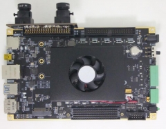
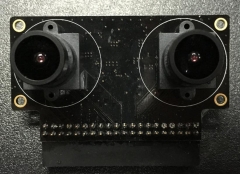
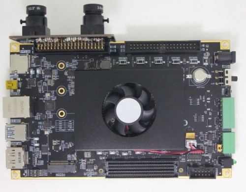
| 1 | Binocular video PL terminal image access | Through THE SENSOR setting of PL, access to binocular visual row field and data information, experience the concept of row field resolution, and understand the characteristics of binocular synchronization. |
| 2 | Single-channel CMOS image Sensor to DP display experiment | Learn the data characteristics of video display, RGB signal characteristics, and the corresponding relationship between data and display through PL terminal code. |
| 3 | AXI bus for VDMA image transmission | Through the interaction between PL side program and PS side, understand the DMA transfer mechanism of video frame transmission, DDR cache, interrupt interactive relationship, continuous image storage and data flow mechanism of algorithm application. |
| 4 | ARM's LWIP network transmission experiment | C program code based on naked running how to completely present UDP/TCP, IP protocol data transceiver, network packet mechanism and transmission mechanism, image network transmission data packet protocol. |
| 5 | Experiment of PC transmission in double channel video network | QT program of upper computer, how to receive image data on the network, realize the analysis of network protocol, data flow caching mechanism, display continuous image display and continuous receive packet interaction. |


 |


